
| Solar Module R&D Roadmap |
 |
| High-efficiency module development |
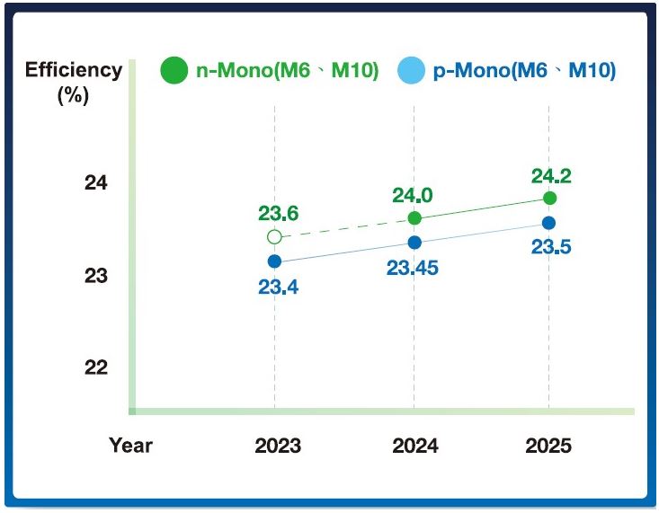
| The conversion efficiency of solar cells directly affects the amount of electricity they can generate, and is also an important factor affecting the cost of solar cells. Currently, the conversion efficiency of traditional single-crystal silicon solar cells is about 23%. By using high-efficiency solar cells and introducing high-reflectivity back sheets and high-transparency EVA materials, the loss can be reduced and the conversion efficiency of module can be improved. |
| Application of soldering technology and materials |
| Crystalline silicon is still the main material for the production of solar cells, and silicon wafers are the main raw material for the production of solar cells. The thickness of the silicon wafer affects the amount of silicon used. The development of thinner wafers can reduce costs and alleviate the pressure on the upstream silicon material supply, but it also increases the difficulty of module manufacture. It requires improving soldering technology and materials characteristics and adjusting to actual production. At the same time, the feasibility of lead-free (Pb-Free) ribbons should be evaluated to meet future market demands. |
| Extend product lifespan |
| Solar power generation systems absorb sunlight and convert it into electricity, and the devices are installed outdoors. They must possess the ability to operate normally under harsh weather conditions. Currently, major companies overseas require solar modules to have a lifespan of about 20~25 years. To meet future market demand, new packaging materials and technologies will be developed, automated equipment will be introduced to improve product quality and reliability. Approaches to consider include research on more durable packaging materials with longer lifespans, or alternative module structures. |
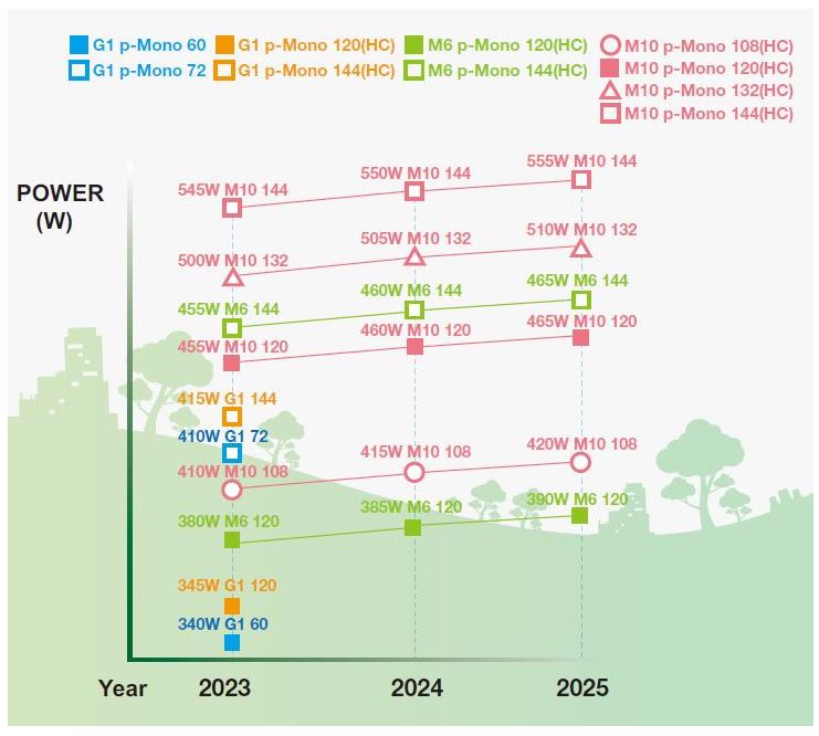
| Improve module power generation efficiency |
| Crystalline silicon remains the main material used in solar cells. The thickness of the silicon wafer affects its usage. The development of thinner wafers can reduce usage and lower costs. It can also alleviate pressure from limited upstream silicon material supply. However, this increases the difficulty in the manufacturing process. The solution is to improve soldering technology and material properties, adjust production practices based on real-world needs, and evaluate the feasibility of Pb-free ribbons to meet future market demand. |
| Solar Cell R&D Roadmap |
 |
| The TSEC solar R&D team consists of professionals with expertise in solar and semiconductor-related fields. With a focus on technological independence, we collaborate with domestic and international equipment and material manufacturers to develop new processes and materials for forward-looking projects. We also execute industry-academia cooperation projects with multiple domestic universities. In 2013, we passed the "Lead New Product Development Plan" of the Industrial Development Bureau of the Ministry of Economic Affairs, and in 2016, we passed the "Energy Industry Technology Project" of the Bureau of Energy. With the cooperation of industry, government, and academia, we believe that there will be substantial achievements in future R&D projects and the development of new types of solar cells. |
| N-type solar cell development |
| N-type wafers have a higher carrier lifetime and toleration of metal contamination than P-type wafers, giving them inherent advantages in developing solar cells. Ordinary N-type solar cells can be highly compatible with our company's existing PERC technology and current processes, requiring no significant investment in research and development costs. Currently, there are three types of ultra-high-efficiency N-type solar cells: Interdigitated Back Contact Solar Cells (IBC), Heterojunction with Intrinsic Thin-Layer Solar Cells (HIT), and Tunnel Oxide Passivated Contact (TOPCon). All three methods can achieve over 24% efficiency, so our company is working on developing the next generation of ultra-high-efficiency N-type solar cells to pursue higher efficiency and more economically viable solar cell products. |
| N-type solar cell development |
| The N-type wafer has higher minority carrier lifetime than the P-type wafer, and has higher durability against metal pollution; therefore, it has the inbuilt advantage to develop solar cell. Most N-type solar cells can use the currently available PERC technology of TSEC, which has high compatibility to the current manufacturing process and can save a lot of development cost. Currently, there are two super high-efficiency N-type solar cell technologies, including “Interdigitated Back Contact Solar Cells” (IBC) and “Heterojunction with Intrinsic Thin-Layer Solar Cells” (HIT). Both of them can achieve more than 24% conversion efficiency. Accordingly, TSEC is trying hard to develop the next-generation super high-efficiency N-type solar cell in order to provide the solar cell products with higher efficiency and economic value. |